Category: Science

XCSoar on a Kobo Touch 2.0 with BlueFly GPS

Hi,

I decided it was time to get a Kobo Touch 2.0 and get XCSoar installed on it, complete with GPS. I chose the Touch 2.0 (Amazon.de).

  1. Buy a Kobo Touch 2.0
  2. Backup the SD Card
  3. You will need to purchase a BlueFlyVario_TTL_GPS_v11. I chose the TTL, as the USB version is prone to breaking the USB connector.
  4. Download and 3D print the cover from ThingVerse.
  5. A Soldering Iron Solder and a few tools.
  6. A spare circuit board to practice your soldering skills. You cannot afford to make a mistake when soldering.
  7. Star Phillips screw driver
  8. 3mm Drill bit
  9. 3M x 6mm bolts and nuts, used to fix the  cover to the case. It is tricky getting the nut to fit in the small gap on the Touch 2.0. I just drill holes on the side of the Kobo and slide the nut in like a coin slot.
  10. Software for the Kobo. You can download it here. That link has pictures and all the software to get the Kobo up and running with XCSoar 6.8.

There are detailed instructions you can follow here.

http://blueflyvario.blogspot.com.au/2014/11/kobo-glo-install.html

The reason for this post, is to compliment the above article with some pictures.


Inventory
Solder Station
Kobo Touch 2.0 Serial Port

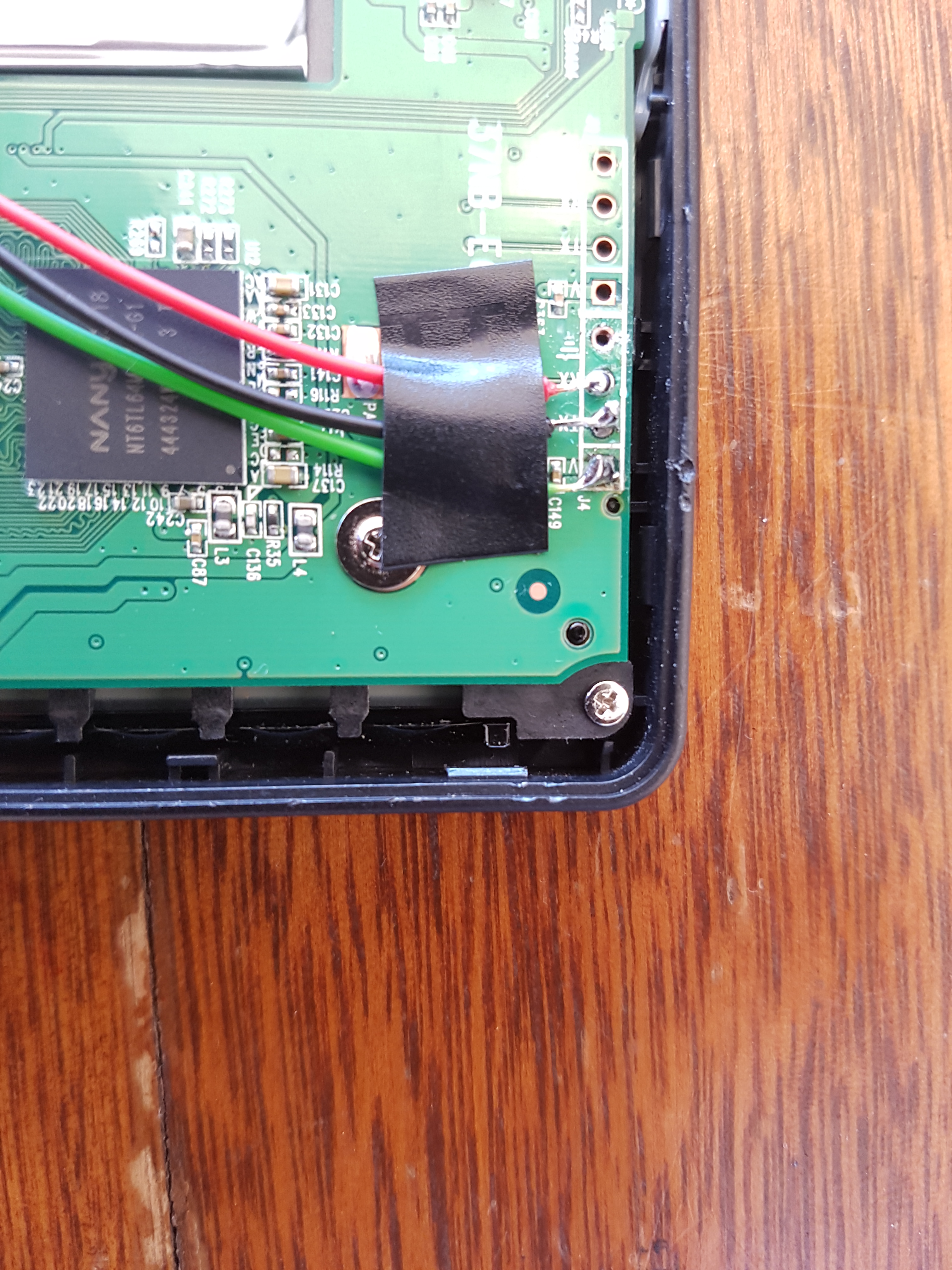
Important: The RX on the Kobo Port goes to TX on the BlueFly. I use the screw to ground the circuit (yellow wire). Green Wire goes to V. Black and Red is TX and  RX on Kobo and switched around on BlueFly.

Soldered To Kobo 2.0
KoboRoot.tgz

Use a Linux Operating System to copy KoboRoot.tgz to the hidden .kobo folder and then reboot the Kobo. I just take out the SD Card, plug it into a machine with Linux or on Windows with a Virtual Machine running Linux (I use Kali Distro).

Customise XCSoar

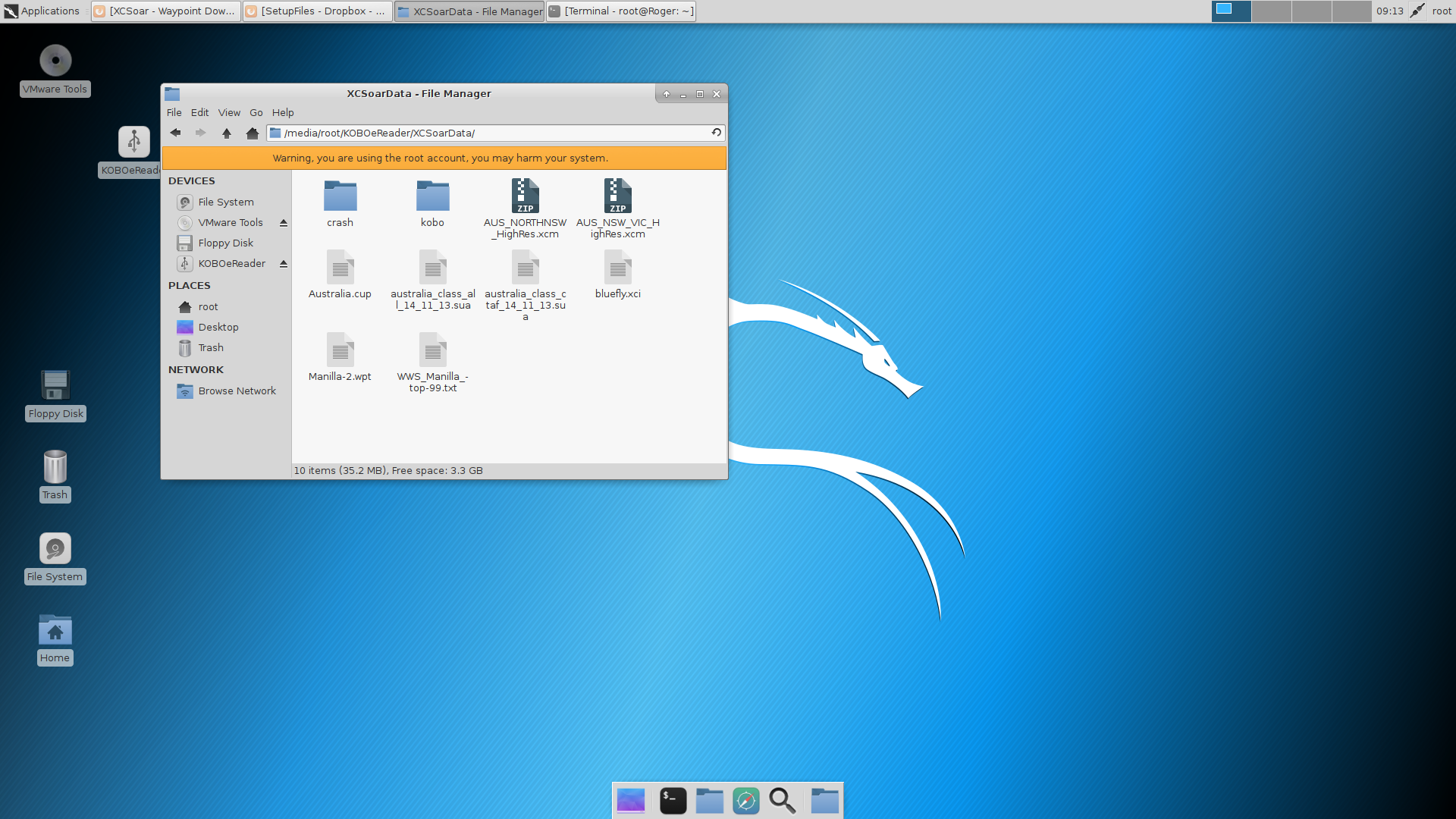
Once rebooted and XCSoar is running, go to Nickle and then plug in the Kobo 2.0, then just copy additional files for XCSoar. E.g. Maps, Waypoints

Device Settings

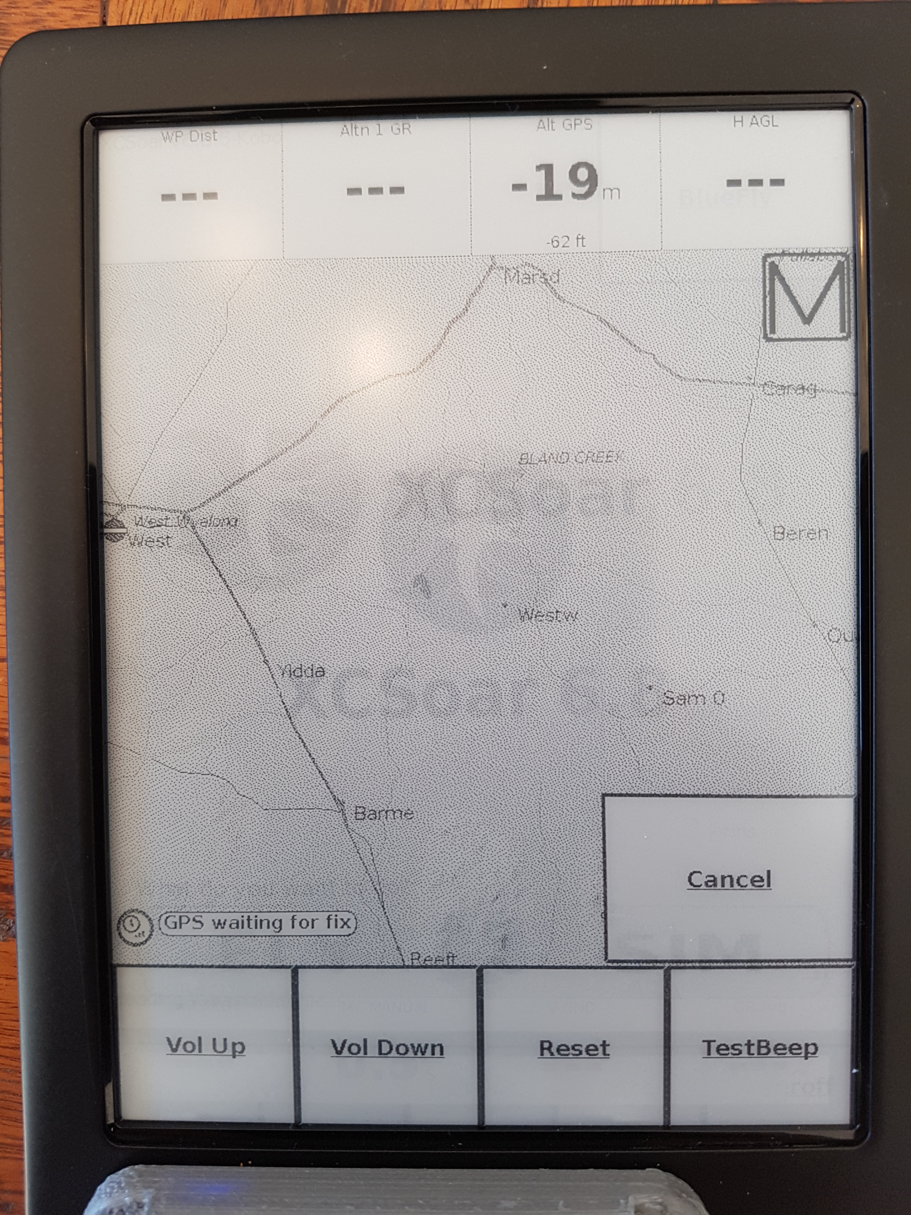
Make sure you go into XCSoar Config -> Devices and set the device settings for the BlueFly Vario. Once done, use the monitor button to check feedback. (Ensure the Vario is turned on, by pushing the button. It will make an annoying sound continuously.)…it was music to my ears.

Events – BlueFly.xci

In XCSoar, register the BlyeFly.xci file as an Event in Language/Input. Ensure advance mode is on. This gives you a cool menu for BlueFly where you can set the volume of the beautiful sound it makes.

bluefly.xci

Go outside, and test your new navigation tool to compliment your flight deck. Happy flying with loads of battery time 🙂

Tips:

I made two holes on the bottom side of the Kobo, to get the 3mm Nuts in, so I could bolt down the cover. Maybe you can get it working with 2mm bolts and nuts….

Only remove the Circuit Board screws. Do not remove the screws that hold the screen in. Leave the screen in the device during the entire modification process.  Keep all wires above the circuit board, else the screen will not function correctly as it relies on a certain amount of pressure around the perimeter of the device. Look carefully under the circuit board, you will see lots of connectors around it. I initially tried to solder from under the circuit board (Easier to solder), but this cause a lot of issues with the screen touch sensitivity.

Nickly and the E-Reader still work after the modifications. If yours does not. Restore the SD card from a backup you made and go through the software modification again. e.g. 1. Copy the koboroot file to .kobo -> Reboot -> Customise XCSoar -> Nickel should work again.

if you ever reset the device with a long press on the power button, it may break Nickel and you can only use XCSoar without the e-reader. The symptom is Nickel will show a black screen.

Advertisement

Calculate Wind Direction and Wind Speed from Wind Vectors

Wind Vectors have a U (Eastward) and V (Northward) Component.

Below is the code in C# to calculate the resultant wind

public struct Wind
    {
        public Wind(float speed, float direction)
        {
            Speed = speed;
            Direction = direction;
        }
        public float Speed { get; set; }
        public float Direction { get; set; }
    }

public static Wind CalculateWindSpeedAndDirection(float u, float v)
        {
            if(Math.Abs(u) < 0.001 && Math.Abs(v) < 0.001)
                return new Wind(0,0);
            const double radianToDegree = (180 / Math.PI);

            return new Wind(
                Convert.ToSingle(Math.Sqrt(Math.Pow(u, 2) + Math.Pow(v, 2))),
                Convert.ToSingle(Math.Atan2(u, v) * radianToDegree + 180));
        }

Test Code

        [TestCase(-8.748f, 7.157f, 11.303f, 129.29f)]
        [TestCase(-4.641f, -3.049f, 5.553f, 56.696f)]
        [TestCase(10f, 0f, 10f, 270f)]
        [TestCase(-10f, 0f, 10f, 90)]
        [TestCase(0f, 10f, 10f, 180f)]
        [TestCase(0f, -10f, 10f, 360f)]
        [TestCase(0f,0f,0f,0f)]
        [TestCase(0.001f, 0.001f, 0.0014142f, 225f)]
        public void CanConvertWindVectorComponents(float u, float v, float expectedWindSpeed, float expectedWindDirection)
        {
            var result = MetraWaveForecastLocationModel.CalculateWindSpeedAndDirection(u, v);
            Assert.AreEqual(Math.Round(expectedWindDirection,2), Math.Round(result.Direction,2));
            Assert.AreEqual(Math.Round(expectedWindSpeed,2), Math.Round(result.Speed,2));
        }

Creativity

The sight of all these people in uniforms does not prime creativity

(Kahneman, D. (2011). Thinking Fast and Slow, Allen Lane 2011 -  Noble Prize 2002 Economic Sciences).

Let’s rethink our culture so that our society can express themselves in a constructive manner and live a more fulfilling life during work hours. To promote conformity and to stifle expression is one of the intrinsic causes of our societies rebellious sub cultures.

So what do suites, ties and school uniforms do for us?  Another social “Etiquette” that hides the true intention of an individual, What are your thoughts?

Musings on Biological Sensors

AFM cantilever probe modes

In stress sensing mode, the reaction from the molecules or sample occur on one side of the cantilever, when there is a change in the total surface free energy, this will the equate to a change in surface stress, which will cause the cantilever to bend. The magnitude and direction of the bending can then be measures using optical means or electrical means by use of lasers and piezo-resistors. The spring constant is inversely proportional to the sensitivity of the device.

In mass sensing mode, the cantilever is excited mechanically, this causes it to vibrate at it’s resonant frequency. The change is mass can be detected by the shift in resonant frequency once a biological molecule attached to the cantilever. Optical or electrical means can be used to measure these shifts.

The above two modes is similar to the contact and non-contact mode on an AFM probe, all methods cause the cantilever to bend either by deflection (Contact Mode), therefore contact mode is similar to stress sensing mode.

Mass sensing mode is similar to Non-contact mode, since here the resonant frequency of the cantilever is used to measure the deflection of the cantilever, where oscillation in the vertical direction are excited and a piezoelectric actuator can be used to pick up the oscillations.

(b) Mass of virus particle

k=0.006 N m-1

Therefore the mass will be the difference in mass changes over the two frequencies.

f1≈1.35 x 10⁶ Hz

f2≈1.42 x 10⁶ Hz

m1= 8.34×10⁻¹⁷ kg

m2= 7.54×10⁻¹⁷ kg

∆m≈8.02×10⁻¹⁸ kg which is the mass of the virus particle.

So a the virus is approximately 8.02 fg (femto grams).

(c)Cantilever modifications

Biding sites may be attached to the cantilever to attract a certain ligand to bind to the cantilever. Gold is a excellent coating to apply to a silicon based cantilever, since this provides a good surface for capture probes to bind to. The cantilever can then be used in stress/mass-sensing mode.

So in summary:

· Create a silicon based cantilever

· Coat with gold

· Attach capture probes to cantilever surface which will match the target ligand

(d)Feasibility and detection (Tuning In)

A cantilever will need to have a high resonant frequency as possible to minimise vibration from external noise. Therefore the lowest resonant frequency of the cantilever should be at least 10 times greater than the highest frequency present in the room. Therefore this specific cantilever’s resonant frequency should be greater than 200kHz.

The feasibility will be to see if the cantilever can vibrate with the range of the resonant frequency required to detect this mass size, which is:

k=0.006 N m-1

m=0.20 x 10⁻¹⁸ kg

f=2.76 * 107 Hz

f≈27.6 MHz
This is well out of the range my one order of magnitude, so the cantilever will not be able to detect a mass of 0.2 fg.

The maximum frequency detected is 1.42 x 10⁶ Hz. It is like trying to tune a radio to listen to microwaves, well close!

However, I wonder if a cantilever has ever been designed to work in amplitude mode, like AM radios?

Musings on CMOS basics

Where did CMOS come from and how did old CMOS chips get made, with large gate lengths, I mean, they now at 30nm in production with Intel

image

image

The reason is a p-n junction is made of a metal for the contact and conduction of electricity, and oxide for insulation to establish a potential difference and a semi-conductor that is doped p-type and another n-type, hence complimentary to each other’s type of doping, to establish drift, diffusion and a depletion region.
They are wide spread in portable devices such as camera’s due to the use of photodiodes which are sensitive to light and can generate current, thus acting as sensitive detectors/ switches of photons, depending on how they are arranges and connected. They are relatively inexpensive to manufacture on a large scale due to the maturity of such devices in the computing industry, where established lithography and fabrication techniques have been perfected over the years and feature sizes have been following Moore’s law.
With slight modifications these transistors can be addressed very easily with an electrical grid system, which is sufficient for transporting and processing the information carried across the wires and establishing an addressing system.

(a) A switch is a simple MOS p-n junction, when there is a bias voltage the switch is on as there is a conduction path between the terminals.
An inverter is two switches connected in series.
A latch is an arrangement of switches that can be set into two different states and provides an electrical output, can be set to either state electrically and is also stable.
Two switches will create an inverter, for CMOS memory this is not practical as it will store the opposite state desired, so a 1 would be a 0 and vice versa and also the output is indeterminate. The solution is 4 switches, so that there are two inverters, one feeding the other, this is what is used to create a memory latch, So sending a 1 or 0 will result in a 1 or 0 being stored on the output and it is determinate, so loss of power will keep the output the same.2
No drain will occur when a switch is open, as the conducting path through the gate terminal has no applied bias applied.

(b) Most of the process steps in the fabrication of CSMOS require photolithography to define areas that are etched or deposited. The photolithography uses a photoresist polymer which is then exposed to UV light and the weaker parts of the resists are washed off, producing a positive or negative depending on the resist used. Resolution of features are limited by these photolithography.
To create CMOS we will need an adjacent p-well and n-well, kitted out with their respective components:

· Gate oxide

· Gate

· Source

· Drain

· P+ Substrate and p layer

· Electrical contacts

One of the most important factors is the gate length and the doping requirements used for these gates.

Some of the challenges involved are:

v Isolating switches from each other

o The p-Type and N-Type switches need to be isolated from each other, this is achieved by Shallow Trench Isolation. The isolation trenches are etched around 400nm deep into the silicon using LPCVD for the sacrificial layer.

o Then a plasma etch is used to form the trenches. This trench is the barrier between switches. There must be no sharp points so the STI etch agent used is HBrO2.

o The trenches must be filled with an insulator, which uses CVD process and the chemical TEOS. The capacitance between each switch has an impact on the speed and power of the chip, so the dielectric constant of the insulator must be as low as possible.

v Defining wells and the role of photolithography

o Wells are the doped silicon which will form the junction with the source and drain contacts. Alternating p/n type wells are masked off by photolithography. Ion bombardment implants donor or acceptor atoms in the silicon surface. The doping stage defines the polarity of the final channel and the sign of the gate voltage used to activate the switch. So the doping concentrations must be correctly applied.

o Width on old chips is around 200nm, new ones will be much smaller now.

v Formation of the Gate Oxide (Insulator)

o The integrity of the gate oxide to act as a insulator is crucial, as electrical breakdown must not occur here. The trick is to control the thickness of the gate oxide to be as thin as possible and use a high quality oxide with high-k dielectrics, due to the capacitance affecting the performance of the device. This oxide is deposited using conventional lithography techniques and uniformity is crucial to a quality gate oxide. The gate length will be in the region of 250nm, which will sit on top of this oxide. The thickness is around 1.2 +- 0.5 nm . With new techniques we looking at 30nm production quality as of 2010.

v Making electrical connections to the switches

o Metals can be deposited using sputter deposition such as PVD. Advanced PVD is needed here to ensure a high degree of directionality, where control of sidewall angle is need for criss-cross grid system, CL2/HBr plasma sis appropriate for this.

This is due to the fact that reducing the gate length will reduce the power consumption of the chip and also allows creating faster gate architectures by increasing the number of transistors in the chip, so smaller feature sizes means more processing power. We need oxides with a High-K dielectrics, hafnium oxide is a promising material since it has a dielectric constant which is 5 times more than silica, this means we can have 5 times the capacitance at the price of the same thickness!

Reverse Bias in Solar Cells

Solar Cell Basics

A photo cell (solar cell) is a p-n junction. A photo cell convert’s light energy into electrical energy and the photons is the current source.

When photons incident the silicon, it either travels through the material if its energy is lower than the band gap energy of the silicon semiconductor (transmission), or is absorbed by the silicon if its energy is higher than the band gap energy , or reflected. If the energy is high enough then an electron-hole pair is produced, and the electron and hole are separated by depletion region of the p-n junction and a current is generated through a connected circuit , since the positive carriers prefer the p-type material and the negative carriers prefer the n-type material, this increases the conductivity of the material.

clip_image001

Diagram showing electron-hole pairs being affected by incident photons.

When no light or photons are incident on the solar cell, then there is a balance between drift and diffusion and the number of electrons and holes are equal between the two regions, and no net current flow is present.

The light detector or solar cell is in fact a photodiode where is will readily conduct current in one direction and hardly at all in the other. With photocells, we need to apply a reverse bias in order to increase the effect of an internal electric field in the junction, thus causing an imbalance of drift and diffusion across the depletion region.

For the photocell, the holes tend to enjoy staying in the p region and the electrons in the n region, reverse bias enhances this tendency. When a stream of photons are absorbed into the silicon and are within the transition region, then electron-hole pairs are formed, then photon generated charge carriers will prefer their n/p type material respectively.

This will result in an additional reverse current through the junction.

In the above diagram, you will notice electron-hole pairs outside of the depletion region, still being able to make the transition, this will be due if they live long enough to slip into the depletion region.

In practise it is preferred to have one of the p-type or n-type materials to be much less than the other to ensure the depletion region extends further on one side only, this ensures. Assuming the p-type is much thinner, then the absorption length of the silicon which is the reciprocal of the absorption co-efficient will need to be tuned with some light doping to ensure the transition region is wider which will increase the probability that incident photons will occur around the transition region where electron-hole pairs are close to the depletion region, else the pairs will recombine due to lower lifetime constants. Therefore the doping requirements will be that one of the material types will have a weaker doping than the other. Also the p-Type material is in contact with the substrate and the initial layers close to the substrate where the electrical contacts are located will have a high doping population P+ the p layer closer to the junction will have a lower doping population p.

Diffusion is responsible for the leakage of charge across the p-n junction when it is experiencing reverse bias due to thermal energy, charge carriers move from high concentration to low concentration. Diffusion pushes minority charge towards the edge of the junction within the depletion region where it is swept across to the other side and becomes a majority charge carrier. See the diagram above, where charge carries are swept across (charge separation). Diffusion is negligible in reverse bias

Drift is where the positive charge will drift in the direction of the positive electric field (negative end of battery) and negative charge will go the opposite way. The total current flowing through the depletion region under reverse biasing is made up of mostly of minority carrier drift.

There are various manufacture processes that can create drift or diffusion dominant diodes depending on the dopant used (Science Direct, 2009)

We will look at the materials used in the next section, that and a battery, where the battery will be used to store the current generated by the solar cell.

The materials required to fabricate a p-n junction are:

· Metal or similar material that is electrically conducting

· Insulator to isolate the voltage applied

· A Semiconductor where the conductivity can be altered by doping and bias voltages

The device to build is in fact a complementary metal oxide semiconductor field effect transistor (CMOSFET). This is where n-type and p-type devices are situated side by side. We will focus on a n-channel silicon MOSFET.

The junction is the region where the n-type and the p-type silicon are in contact with each other.

clip_image002[4]
Diagram representing a p-n junction

clip_image003 

As we can see from the above, when in equilibrium the electrons “diffuse” across and combine with the holes; this area is known as the depletion region.

When a current is applied by making the p-type more positive and the n-type more negative, it will flow readily in one direction (Forward Bias) but not in the other (Reverse Bias).

To form a pn junction different conductive regions must be adjacent to each other and a rapid spatial change in the dopant species from donor to acceptor must be created.

The reverse bias enhances the large field potential in the device and thus charge carriers are rapidly accelerated to the respective anode and cathode electrodes, thus contributing to the current.

What about forward bias?

In forward bias, the internal field would essentially be destroyed and the charge carriers would move very slowly and hence your solar cell would be less effective.

Furthermore applying a forward bias would temporarily reduce or destroy the junction as it would induce carriers to move in the same direction as the diffusive flow, thus smoothing out the carrier differences.

Musings on Cantilever Stiffness in Electron/Atomic Force Microscopes

The equation for stiffness is:
clip_image002

Where a is the width, b is the thickness and l is the length. This has an effect on mass which in turn will affect resonant frequency.

However, these cancel each other’s effect on stiffness if increases simultaneously. So something else besides stiffness must be responsible for the benefits of ATM work, which is indeed the relationship between mass and resonant frequency.

However a high stiffness cantilever in Non-Contact mode ensures the attractive force between the surface and the tip do not cause the cantilever to “bend” and succumb to the attractive force.

Short and thin cantilevers made from Silicon on Oxide wafers have a low force constant which is suitable for probing, especially soft samples when working in Non-Contact/tapping mode, since excessive force is not applied to the surface being scanned.

Angular velocity can be used to obtain the Frequency:

fo0/2π

The angular velocity equation for a cantilever is:
clip_image004

From the above equation we can see that smaller values for length and thickness of the cantilever structure then the higher the frequency will be.

The intrinsic high resonance frequency is most useful in Non-contact/tapping mode, since the tip is not in contact, and the oscillation induced on the tip by the piezoelectric actuator allows the tip to “linger” a little longer closer to the surface. Lower frequency modes means the tip will spend less time at the closest point to the surface in the oscillation cycle. This ensures that effects of vibrations from the surroundings are minimised and a high image acquisition rate (due to increasing the time the tip is closest to the surface). Thermal noise is also reduced.

Fabrication of short and thin silicon cantilevers for AFM with SOI wafers

clip_image002

Sensors and Actuators A: Physical, (2006)

Step 1: Forming the handles

Stage (a) Preparation

Silicon wafers with a <1 00 > orientation (Horizontal Alignment) are used and the top most layer of Silicon will be used to form the tip.

Oxide layer is deposited between two layers of silicone and also at the top and bottom of the wafer by thermal oxidation at 1000 ⁰C.

The thermal oxide layers act as a mask at the handle side and at the top side where the tip will be defined, it also protects the silicon layer that will become the cantilever when the trenches/cleaving lines (T, C) are formed.

Stage (b) Etch Trenches

The trench lines are formed using convention lithographic techniques, by forming a photoresist on the bottom of the wafer.

Chemical hydrofluoric wet etching is used to open the sections of the oxide layer on the exposed regions of the photoresist, this etch technique cannot be used on the silicon itself as the rate of etching is too slow.

Once the oxide layers are removed from the trench pattern, then Tetra-methyl ammonium hydroxide (TMAH) wet etching is used on the Si handle layer. TMAH is better than Potassium hydroxide as KOH will destroy the oxide layer which acts as a mask here.

The etching depth is controlled by duration of the wet etch, the trenches are etched in around 12 hours and the cleaving (C) in a shorter time period to have a reduced depth as compared to the T.

Note that TMAH does not etch the oxide layer and hence this layer is left in the trench (T).

Step 2: Defining the cantilevers

Stage (c)

Conventional lithographic techniques are used to pattern the trench area of the device layer side, so that accurate alignment of the cantilever with the respect to the trench (‘T) can be achieved.

· KOH wet etching is used to etch the cantilever in a 60⁰C water bath (E)

The depth of etching is controlled by the duration and reactants used.

Stage (d)

· The cantilever mesa (M) and (E) are then etched together, a suitable photoresist and photomask is used to ensure some of the oxide layer is not etched using isotropic etching.

This stage ensures the cantilever is strong enough to withhold tensions and stress caused by spinning photoresist and other subsequent steps, thus ensuring the alignment is accurate throughout the process.

Step 3: Forming the tips and cantilevers together

Stage (e)

· KOH wet etching is used.

· The etching rate will be uniform, therefore when the (E) part of the device is totally etched off, the etch process is topped immediately. This provides the necessary sign to stop etching and will ensure a thin cantilever is left as the (M) part is thicker than the (E) part.

· Thermal oxidation can be used to sharpen the tip, reduce thickness and balance the stress in the cantilever. The above process is easily to control due to several hours needed for etching and oxidising! Therefore quantitative monitoring processes can be established during production.

Atom Force Microscope Tip

clip_image002

Dip-Pen illustration (Dip-Pen Lithography, 2008)

The tip of an Atomic Force Microscope is coated with a thin film of thiol molecules that are insoluble in water but react with a gold surface.

When the device is exposed to an atmosphere with high saturation of water vapour, then tiny water molecules will condense between the tip of the microscope and gold surface. Surface tension ensures there is a constant fixed distance between the tip and the surface, as the tip moves across the surface, a bridge is formed and the thiol molecules can move onto the gold surface, where they stay fixed due to a chemical reaction.

This technique is slow and cumbersome and can however create features a few nanometers across. So this device can even build smaller wires that are only one atom wide.